So it’s been a bit of a long time since I blogged on WordPress, but I am back again. Please bear with this specific blog as it is a work in progress.
Also apologies for layout glitches as I am getting used to the new blocks editor on WordPress before they retire the old WYSIWYG editor.
I had an old WG12864a display in my components box and I wanted to get it working with one of my PSoC development boards.
Sadly the magic grey smoke has escaped from both the display and the development board when an errant flying wire contacted with something it should have stayed away from.
Never fear this handy trader on E-Bay had a similar Text and Graphic Display using the ST7920 display driver.


There are lots of Arduino sketches for these types of display, but not much for Cypress PSoC 4 & 5 devices. As you will all know by now Crusty of “Crusty Hacks” likes the programmable hardware PSoC chips use. Using programmable hardware to handle what would b a “bit bashing” fest on a micro makes an awful lot of sense to me and being able to do things in parallel without intervention of the embedded micro just seems right.
So there are a number of options when using this display 4 bit, 8 bit and SPI modes of communication
- 4 bit mode will use 8 pins on the controller,.
- 8 bit uses 12 pins.
- SPI uses 4 pins.
There are I2C breakout boards that provide a I2C serial to parallel mode for these displays, which will use only 3 pins from the controller. SPI uses 3 but I have opted to add one extra pin to allow for a hardware rest line.
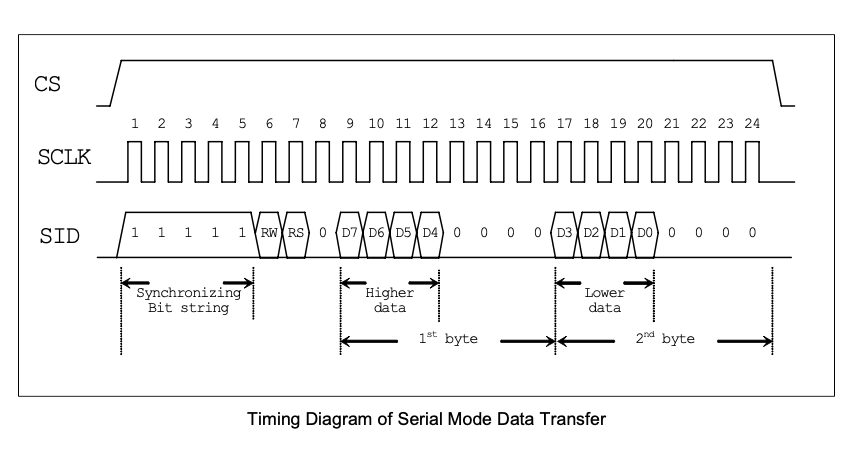
The SPI data that is sent to the display is write only and is made up of 24 bits of data, only 9 bits of data will change in any 24 bit data frame, RW bit (Read/Write) will always be write as there is no read capability in SPI mode. Only the RS bit (Command or Data) and the 4 Higher and 4 Lower bits of data are going to change in any data frame.
Diagram from Sitronix data sheet.
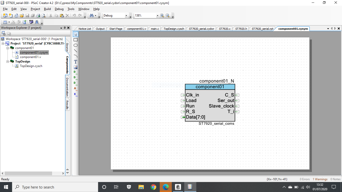
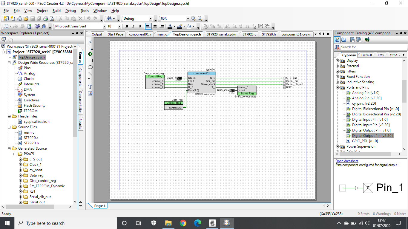
It’s time to build a custom component for my Cypress PSoC 5 development board.
I am going to learn enough Verilog HDL (High Level Description language) to get Cypress Creator Warp Verilog to synthesise the component for me.
The component is going to need CLOCKS
- An input clock
- A data clock to drive the data out one bit at at time from the SID output
- A SCLK output that is 90 degrees out of phase with the data stream so the display knows when to read the data.
The component is going to need inputs.
- 8 data inputs.
- A SCLK output that is 90 degrees out of phase with the data stream so the display knows when to read the data.
The component is going to need inputs.
- 8 data inputs.
The component is also going to need outputs.
- outputI SCLK output
- 1 CS output
The component is also going to need control inputs and outputs
- 1 Load control line.
- 1 Run control line.
- 1 Frame sent or ready to load control line.
Now this is looking like a lot of inputs and outputs, but the component being designing is in the PSoC chip and only has the SID, SCLK and CS outputs coming out of the physical pins of the PSoC 5 chip.
Screen Shot of the component thats needed
 Next thing to do is think about what we want to happen.
- Take an input clock make two clocks in step with each other but 90 degrees out of phase, Not as difficult as you might think only 2 d flip flops and some inverters. Diagram from


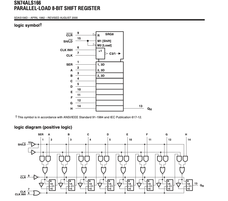
- The parallel load serial shifter element is needed but it’s going to be 24 bit long and not 8 bit as per the diagram taken fromTexas Instruments Data sheet.
 There is a slight flaw in my decision to use Warp Verilog to make my component
Warp Verilog needs you to be conversant with writing Verilog already, you input the Verilog just as you might write a C file. The error messages when Warp copies are not very helpful Warp has no RTL diagrams or Schematic diagrams and no testbed feature.
I have hit this before and have found a way to use the old but excellent Xilinx FPGA’s ISE design suite to write Verilog instructions that can be cut and pasted in to the Creators Warp Verilog file. The reason I use ISE is that it has an embedded help which has snippets of code for just about every element that you will use in your Verilog code, which you can copy and paste. It also has a schematic capture option which is not quite as useful for what we are going to do.
ISE is a big programme and you need a fairly fast PC, however you are not working in the cloud. While learning you can keep recompiling as often as you need to get rid of all the syntax errors and logic errors you may have. Now half the learning cycle of Verilog or even (VHDL) is understanding the error messages during synthesis. Whats “SYNTHESIS” in my simple terms getting your text description of the circuits components and their timing interaction transferred into logic packages the the FPGA vendor can assemble in the undedicated logic on their chip. This is where the fun starts take the simple logic function that we will use in our component.
This will synthesise into the following schematics
Registerter-transfer level RTL schematic.

Technology schematic
Technology schematic

So this is what Xilinx would fabricate the circuit as.
Interestingly the Xilinx Technology design has got rid of the simple flip-flops and used a flip-flop with a clear and reset. Similarly when we use the Verilog description in the Creator WARP file then we are told that WARP will parse the Verilog description and utilise predefined components in WARP to generate our design.
Which is why I put a logic analyser on the outputs and inputs of a custom component so that I can see that the design performs as expected.

The Module used in a Creator Schematic design
The Verilog HDL that sits inside the component above
include “cypress.v”
//`#end` — edit above this line, do not edit this line
// Generated on 06/23/2020 at 12:10
// Component: component01
module component01 (
output reg C_S,
output Ser_out,
output reg Slave_clock,
output reg T_i,
input Clk_in,
input [7:0] Data,
input wire Load,
input R_S,
input wire Run
);
//`#start body` — edit after this line, do not edit this line
// Your code goes here
reg [23:0] shifter;
assign Ser_out = shifter[23];// set this as the output buffer
reg running;
reg [4:0] count; //set up the incrimenting counter for counting bits shifted
//**************take clock in signal divide by 2 and generate two clocks shifted by 90 degrees************
reg a;
reg b;
wire Clk_0;
assign Clk_0 = a;
wire Clk_90;
assign Clk_90 = b;
always @ (posedge Clk_in)
begin
a <=~a;
end
always @ (negedge Clk_in)
begin
if(running == 1’b1)
begin
b <= ~b;
Slave_clock <= Clk_90;
end else
begin
Slave_clock <= 1’b0;
end
end
//*****************************************************
always @ (posedge Clk_0)
begin
if(Load == 1 )
begin
shifter[23:19]<=5’b11111;//low value to start in bit 24 followed by 5 framing ones
shifter[18]<=1’b0;
shifter[17]<=R_S;
shifter[16]<=1’b0;
shifter[15:12]<= Data[7:4];
shifter[11:8]<=4’b0000;
shifter[7:4]<= Data[3:0];
shifter[3:0]<=4’b0000;
T_i <=1’b0;
C_S <=1’b0;
count <=5’b00000;
running <=1’b0;//set slave clock off
end
else
if(Run == 1 )
begin
if(count == 0)
begin
C_S <= 1’b1;// set Chip select high
running <= 1’b1;//set up the reg to start Slave_clock //output(always(negedge Clk_in)statement
T_i <= 1’b0;
count <= count + 1;//increment count so this only act s once
end
if(count >= 1 & count <=23)
begin
shifter <= shifter <<1;// move bits to the right and out to output with shifter[24} as Ser_out pin
count <= count +1;//keep a count of how many times shift happens
end
else if(count > 23)//sent all the serial bits
begin
C_S <=1’b0;//Chip select goes low
T_i <=1’b1;
running <= 1’b0;//set up the reg to stop Slave_clock output(always(posedge Clk_in)statement)
end
end
end
//`#end` — edit above this line, do not edit this line
endmodule
//`#start footer` — edit after this line, do not edit this line
//`#end` — edit above this line, do not edit this line
Had a bit of trouble adding a testbed so below is the screenshot for the the initialising sequence for the display.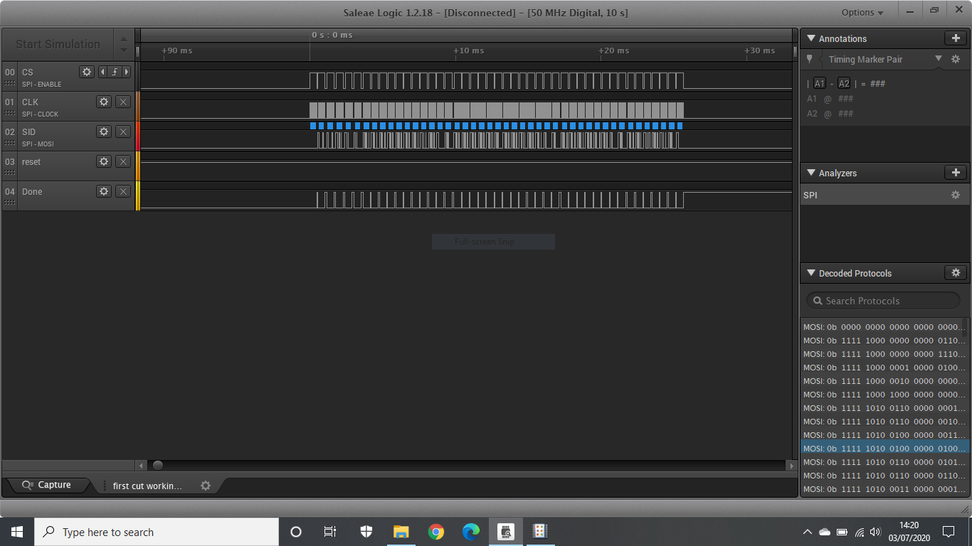 And here is the screen shot of one 24 bit serial frame sent to the display.
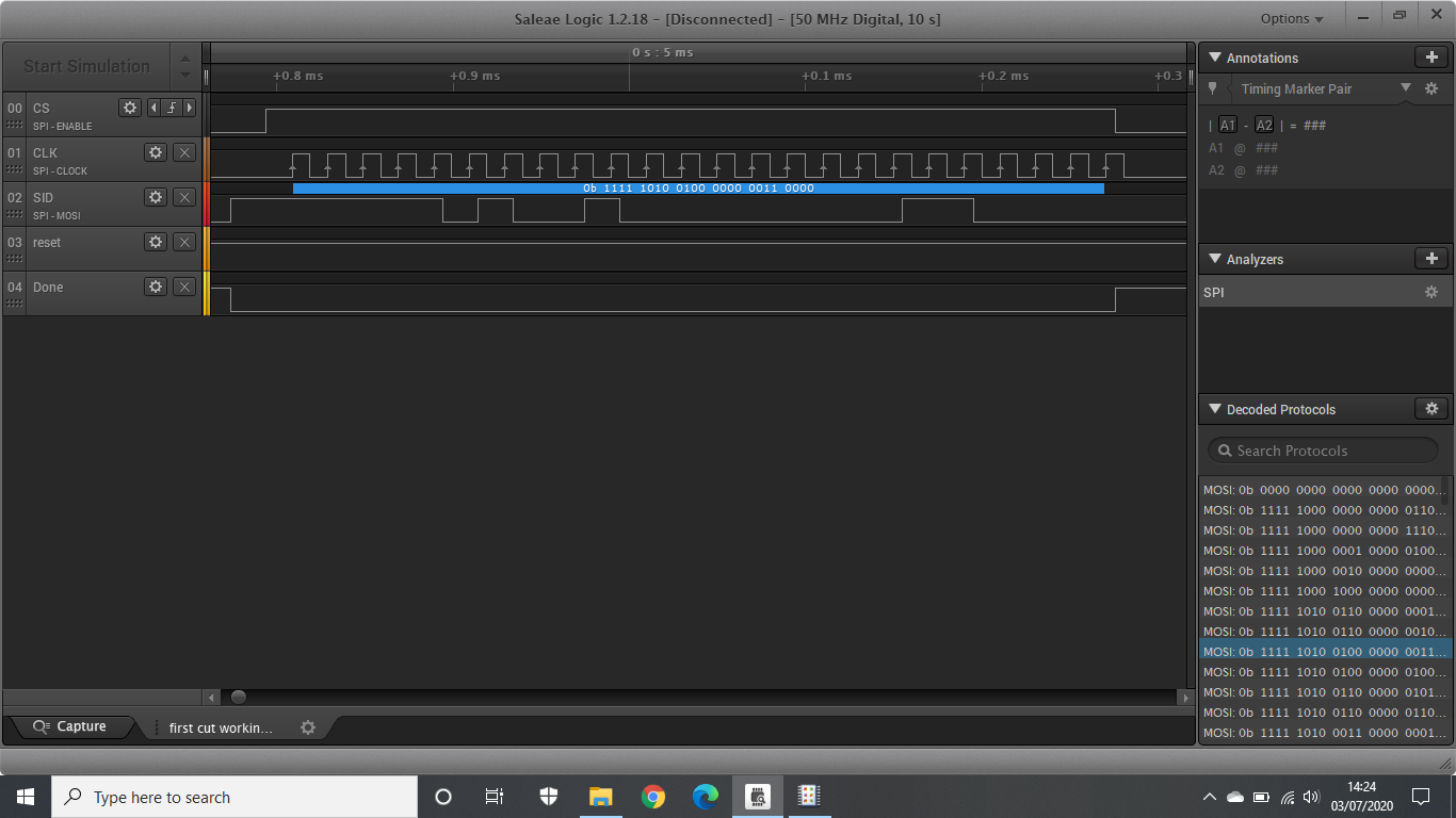
Now the H file of what will become the API for the module
#include <project.h>
#ifndef __ST7920_H__
#define __ST7920_H__
#include <stdbool.h>
#include <string.h>
#define ACTIVE 1
#define INACTIVE 0
#define COMMAND 0
#define DATA 1
#define RESET_ACTIVE 0
#define RESET_INACTIVE 1
void ST7920_hard_reset();
void ST7920_basic_instruction();
void ST7920_disply_clear();
void ST7920_command_data( uint8 command_data, uint8 c_d_byte);
void ST7920_write_character(uint8 line, uint8 position ,char character);
void ST7920_write_string(uint8 line, uint8 position ,char *string_out);
#endif
/* [] END OF FILE */
The C File that will become the API of the Module
#include <ST7920.h>
int modifyBit(int x, unsigned char position, bool newState)
{
int mask;
int state;
mask = 1 << position;
if (newState == 1) state = 1; else state = 0;// relies on true = 1 and false = 0
return (x & ~mask) | (-state & mask);
}
void ST7920_command_data( uint8 command_data, uint8 c_d_byte)
{
// bits 0load, 1run, 2R_S
//should cope with what ever clock is set for the serial component
uint16 command_delay = 1600;//longest delay used
// while(Shift_done_status_Read() == 0)
{
//do nothing a previous shift is in process
};
Disp_control_reg_Write(0b00000000);//shifting has stopped now, control reg value should hold component stopped
Data_reg_Write(c_d_byte);//set up the c-d_byte to send out
if (command_data == COMMAND)
{
Disp_control_reg_Write(0b00000001);//load with register select bit 2 as command 0
while(Shift_done_status_Read() != 0){}; // wait for the load to complete slow clock shown by Ti output on comonent going high
Disp_control_reg_Write(0b00000010);//run, register select dont care in run mode as loaded
if(c_d_byte == 0b00000010)
{
command_delay = 1600;//clear screen takes a long time
}
else
{
command_delay = 200;//most other commands
}
};
if (command_data == DATA)
{
Disp_control_reg_Write(0b00000101);//load with register select bit 2 as data 1
while(Shift_done_status_Read() != 0){}; // wait for the load to complete slow clock Ti of component going low
Disp_control_reg_Write(0b00000110);//run, register select dont care in run mode as loaded
command_delay = 50;//delay for data to be stored.
};
while(Shift_done_status_Read() == 0){};//do nothing until shift complets
CyDelayUs(command_delay);//delay for display processor to complete action
};
/*
void ST7920_data(uint8 data_byte)
{
// bits 0load, 1run, 2R_S
Disp_control_reg_Write(0b00000000);//should hold stopped
Data_reg_Write(data_byte);//set up the command byte to send out
Disp_control_reg_Write(0b00000101);//load with register select bit 2 as data 1
Disp_control_reg_Write(0b00000110);//run,RS x dont care register select in run mode as loaded
while (Shift_done_status_Read() == 0)//check to see when all serial data sent
{
};
CyDelayUs(2000);//delay for data to be stored.
};
*/
void ST7920_basic_instruction()
{
ST7920_command_data(COMMAND,0b00000110);//cursor moveto the right DDRAM address counter (AC) plus 1
ST7920_command_data(COMMAND,0b00001110);//Display on,cursor on,blink off
ST7920_command_data(COMMAND,0b00010100);//cursor mover right by 1 position
ST7920_command_data(COMMAND,0b00100000);//4bit bus (should be dont care basic instruction set
};
uint8 ST7920_set_DDRAM_address(uint8 line, uint8 position)
{
uint8 DDRAM_add =0;
switch(line)
{
case 0 : DDRAM_add = 0x80; break;
case 1 : DDRAM_add = 0x90; break;
case 2 : DDRAM_add = 0x88; break;//yes correct data sheet wrong
case 3 : DDRAM_add = 0x98; break;//yes correct data sheet wrong
};
DDRAM_add = DDRAM_add + (position / 2);
ST7920_command_data(COMMAND,DDRAM_add);
return(DDRAM_add);
};
void ST7920_write_character(uint8 line, uint8 position ,char character)
{
ST7920_set_DDRAM_address(line,position);
ST7920_command_data(DATA,character);
};
void ST7920_write_string(uint8 line, uint8 position ,char *string_out)
{
uint8 count = 0;
ST7920_set_DDRAM_address(line,position);
for(count = 0; count <= strlen(string_out); count ++)
{
ST7920_command_data(DATA,string_out[count]);
};
};
void ST7920_hard_reset()
{
RST_Write(0);
CyDelay(100);//wait
RST_Write(1);
CyDelay(200);//wait
ST7920_command_data(DATA,0b00000000);//reset the serial component to quiescent state dummy data send
ST7920_disply_clear();
};
void ST7920_disply_clear()
{
ST7920_command_data(COMMAND,0b00000001);//display clear
};
/* [] END OF FILE */
Had a bit of trouble adding a testbed so below is the screenshot for the the initialising sequence for the display.And here is the screen shot of one 24 bit serial frame sent to the display.
Now the H file of what will become the API for the module
#include <project.h>
#ifndef __ST7920_H__
#define __ST7920_H__
#include <stdbool.h>
#include <string.h>
#define ACTIVE 1
#define INACTIVE 0
#define COMMAND 0
#define DATA 1
#define RESET_ACTIVE 0
#define RESET_INACTIVE 1
void ST7920_hard_reset();
void ST7920_basic_instruction();
void ST7920_disply_clear();
void ST7920_command_data( uint8 command_data, uint8 c_d_byte);
void ST7920_write_character(uint8 line, uint8 position ,char character);
void ST7920_write_string(uint8 line, uint8 position ,char *string_out);
#endif
/* [] END OF FILE */
The C File that will become the API of the Module
#include <ST7920.h>
int modifyBit(int x, unsigned char position, bool newState)
{
int mask;
int state;
mask = 1 << position;
if (newState == 1) state = 1; else state = 0;// relies on true = 1 and false = 0
return (x & ~mask) | (-state & mask);
}
void ST7920_command_data( uint8 command_data, uint8 c_d_byte)
{
// bits 0load, 1run, 2R_S
//should cope with what ever clock is set for the serial component
uint16 command_delay = 1600;//longest delay used
// while(Shift_done_status_Read() == 0)
{
//do nothing a previous shift is in process
};
Disp_control_reg_Write(0b00000000);//shifting has stopped now, control reg value should hold component stopped
Data_reg_Write(c_d_byte);//set up the c-d_byte to send out
if (command_data == COMMAND)
{
Disp_control_reg_Write(0b00000001);//load with register select bit 2 as command 0
while(Shift_done_status_Read() != 0){}; // wait for the load to complete slow clock shown by Ti output on comonent going high
Disp_control_reg_Write(0b00000010);//run, register select dont care in run mode as loaded
if(c_d_byte == 0b00000010)
{
command_delay = 1600;//clear screen takes a long time
}
else
{
command_delay = 200;//most other commands
}
};
if (command_data == DATA)
{
Disp_control_reg_Write(0b00000101);//load with register select bit 2 as data 1
while(Shift_done_status_Read() != 0){}; // wait for the load to complete slow clock Ti of component going low
Disp_control_reg_Write(0b00000110);//run, register select dont care in run mode as loaded
command_delay = 50;//delay for data to be stored.
};
while(Shift_done_status_Read() == 0){};//do nothing until shift complets
CyDelayUs(command_delay);//delay for display processor to complete action
};
/*
void ST7920_data(uint8 data_byte)
{
// bits 0load, 1run, 2R_S
Disp_control_reg_Write(0b00000000);//should hold stopped
Data_reg_Write(data_byte);//set up the command byte to send out
Disp_control_reg_Write(0b00000101);//load with register select bit 2 as data 1
Disp_control_reg_Write(0b00000110);//run,RS x dont care register select in run mode as loaded
while (Shift_done_status_Read() == 0)//check to see when all serial data sent
{
};
CyDelayUs(2000);//delay for data to be stored.
};
*/
void ST7920_basic_instruction()
{
ST7920_command_data(COMMAND,0b00000110);//cursor moveto the right DDRAM address counter (AC) plus 1
ST7920_command_data(COMMAND,0b00001110);//Display on,cursor on,blink off
ST7920_command_data(COMMAND,0b00010100);//cursor mover right by 1 position
ST7920_command_data(COMMAND,0b00100000);//4bit bus (should be dont care basic instruction set
};
uint8 ST7920_set_DDRAM_address(uint8 line, uint8 position)
{
uint8 DDRAM_add =0;
switch(line)
{
case 0 : DDRAM_add = 0x80; break;
case 1 : DDRAM_add = 0x90; break;
case 2 : DDRAM_add = 0x88; break;//yes correct data sheet wrong
case 3 : DDRAM_add = 0x98; break;//yes correct data sheet wrong
};
DDRAM_add = DDRAM_add + (position / 2);
ST7920_command_data(COMMAND,DDRAM_add);
return(DDRAM_add);
};
void ST7920_write_character(uint8 line, uint8 position ,char character)
{
ST7920_set_DDRAM_address(line,position);
ST7920_command_data(DATA,character);
};
void ST7920_write_string(uint8 line, uint8 position ,char *string_out)
{
uint8 count = 0;
ST7920_set_DDRAM_address(line,position);
for(count = 0; count <= strlen(string_out); count ++)
{
ST7920_command_data(DATA,string_out[count]);
};
};
void ST7920_hard_reset()
{
RST_Write(0);
CyDelay(100);//wait
RST_Write(1);
CyDelay(200);//wait
ST7920_command_data(DATA,0b00000000);//reset the serial component to quiescent state dummy data send
ST7920_disply_clear();
};
void ST7920_disply_clear()
{
ST7920_command_data(COMMAND,0b00000001);//display clear
};
/* [] END OF FILE */
I have just started on the basic C functions to support the graphic display and this will have a 5*7 ascii font.So given the Covid19 keeps me indoors there should be some more code added to this blog along with basic lines squares and circles, which actually means adapting previous code for a SSD1331 display. So I will try not to keep you waiting too long.
I have just started on the basic C functions to support the graphic display and this will have a 5*7 ascii font.So given the Covid19 keeps me indoors there should be some more code added to this blog along with basic lines squares and circles, which actually means adapting previous code for a SSD1331 display. So I will try not to keep you waiting too long.
Getting text to format in the correct position on a line
Text should be easy to send except that the display has really been set up to display Chinese characters which are 16 x 16 character fonts, but will display two 16 * 8 ascii characters which means there are only 8 write locations in a 16 character line.
I took the easy way out to handle formatting a line of text, especially as you can not read memory from the display in serial mode. I am using four arrays of 16 char elements to represent line0 ,1 ,2 ,3 of the text display. On each edit of a line I edit the Array, to position the characters being sent and then just send the whole line array to the display. This way I can edit numbers theatre scaling up and down without affecting the text in the line. Oh there was a “got yer ” in the data sheets memory map for text line start address which I have itemised in the software driver for outputting text. Which is why I have been so slow in putting a video of the text in the blog.
ST7920 Graphics addressing is wierd.
THE GAMES AFOOT.
AS for graphics yet again this has driven me to distraction, as the data sheet is not that clear how the blocks of 16pixels are stored to the screen.
It turns out that the display only has a Vertical Y address of 32 lines and the Horizontal X address is 8 blocks of 16 bits for the upper half of the display. For the lower half you need the Vertical Y (0-63 lines) as modulo of 32 and then add 8 to the Horizontal X address blocks of 16bits.
along the way the MSB needs to be the LSB in the 16 bits of a block. I will include the hack of my code for the graphics and text tomorrow with a video of it in action.
I very nearly have enough of this working now to go onto my next part of the project which is the next blog


