MINI LATHE MOTOR UPGRADE TO 500 WATT BRUSHLESS

Featured


MINI LATHE MOTOR UPGRADE

MINI LATHE 500 WATT BRUSHLESS MOTOR

HOW TO HACK THE ELECTRONIC STEPPER CONTROLLER

UPGRADING MY LATHE TO A 500 WATT BRUSHLESS INDUSTRIAL SEWING MACHINE MOTOR OF THE CHEAPER E-BAY VARIETY.

THE STANDARD LATHE 

The Amadeal CJ18A 7×14 Mini-lathe 

BEAR WITH ME AS I UPGRADE THIS POST AS THE GOOGLE BLOG I WAS USING DOES NOT APPEAR IN SEARCHES so if you are here I will be getting the links and a better document together in the next days.

Mine is about 10 years old and it has been turning parts on and off during this time, but with a fairly poor surface finish and fair amount of noise. Last year the very stiff  Hi/Lo gear change got to the point of not being able to change speed and had luckily got stuck in Lo.

Knowing that the standard lathe comes with a plastic Hi/Lo gear set installed in the headstock, I ordered a new headstock from Amerdeal with a metal Hi/Lo gear set. 

After a year of sitting on the bench I have got around to stripping the old headstock off the lathe and replacing it with the new headstock.

This change went well after following the U-Tube videos and so I should be happy? 

I have no hearing in my left ear and 3/4 standard hearing in the right ear, so noise has to be loud for me to complain. 

However I can tell you those metal gears are noisy and you should use ear defenders when working on the lathe with this gear set. They also rattle a lot, all in all not what I was looking for. If you do use them then make sure to pack plenty of grease around them. May be a bit unfair as after about 2 hours of turning parts for the new lathe motor these metal gears have polished in and are less noisy than they were to start with. I still think they need to run in a dipping oil bath.

I now have a spare headstock and a mainly working lathe. My lathe has ben getting issues with the motor and motor drive controller ( a known problem and more so in countries with 120 Volt AC) therefore it is time to make my own alterations to the drive for this lathe.

A lot of these lathes are now sold with Brushless high power stepper motors and new speed controllers and with no Hi/Lo gear box. 

How difficult is it to upgrade this standard lathe to a brushless version?

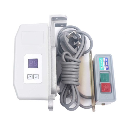
This is a very good link on how to do it , but it is not how I have progressed my upgrade. The Industrial sewing machine motor kit used in the video, is almost unobtainable at the moment in the UK. Similar motors and control panels are available for less money on E-Bay and as I am always game for the low cost option, I bought this industrial sewing machine motor and controller. Link to my industrial sewing machine motor kit

Below are two images from this traders web site and show what I got for my money. The trader was great and sent me a PDF of the instruction manual as I was worried that I might not be able to run the motor in reverse. 

While looking at the links, have a look at a this link that looked at reverse engineering the motor controller See the problems on hacking the electronics .

Mounting the motor and controller.

Unlike the more expensive motor version in the video the mounting bracket on this motor does not come off.

So this is a blog on how I have adapted the motor to fit my lathe.

I have a spare headstock at the moment with the seized Hi/Lo gear set so I am going to convert this to the new motor drive with minimal distance between the headstock shaft and new motor.I thought it would be a good thing to replace the standard headstock bearings with taper roller bearings and there are lots of great videos on how to do this on the web. One video is so brutal when removing and fitting the bearings, it’s a wonder the headstock casting did not break. Breaking out the original bearings is not helped by the very rough finish of my headstock shaft and I must admit that I too had to be fairly brutal in removing the original bearings. I also had more problems with the removal of the change gear shaft bearings than the headstock shaft. I have spare bearings but the shaft will need some machining to replace them. I am not sure if I am going to need this change gear shaft yet, as I want to direct drive onto the headstock shaft.

Shrink the headstock shaft.

Before fitting the new headstock bearings I lightly honed the shaft in the bearing seating locations and reduced the shaft diameter by enough between the bearing seating points to allow the front bearing to travel the length of the shaft with less stress during fitting. I also put the shaft in the deep freeze overnight (plastic bagged to keep oil away from the food and the good lady away from my neck). With the shaft at minus 18 degrees centigrade and the bearings at 30 degrees centigrade, I was able to drive the bearings onto the shaft with a plastic drain pipe. The pipe is only just larger than the shaft itself so is a great way to drift the bearing bush onto the shaft. I wondered if it would take the hefty blows with a club hammer when driving the bearing on, but it took all the pressure exerted and got the front bearing seated after which I was able to follow up putting on the back bearing.
The headstock casting has quite a few holes already drilled into its surface which won’t be used as the control electronics have been removed. So can I use these threaded holes to attach my new motor. I like this idea as the old motor is at the back of the lathe, built in to the lathe bed and difficult to work on, especially as the lathe is heavy to turn round on a narrow bench in my shed.
You can drill the headstock casting, a lot of people have (putting in oiler points) but beware of where you are drilling!!!!

YOU ARE LUCKY AT THE START OF A PROJECT IF YOU HAVE ALL THE PARTS TO HAND.

I do not a present have the timing gears and timing belt that will form my new drive train.So it will be some weeks before I am can post some pictures of my hardware hack. I am having to exhibit some patience while waiting for the timing gears and and drive belt to arrive from three different suppliers to get this refurbished headstock turning again. So hang in there and at some time I will be able to post a video of the new headstock and motor drive. I am also working on a method to mechanically set the motor speed probably Servo or small linear stepper motor, it might even be a bicycle handlebar gear lever as they can have up to 8 detents to act as various speed settings. Thoughts to ponder.

Can Crusty make a safe hack into the electronics.

I think I have a simple, safe hack using an Arduino but isolation from the controllers electronics is essential.I have the inkling of any idea to hack into the electronic control and will post my findings as they happen.
Lets consider the controller
Below is the main board, the lever moves a magnet across a hall effect transistor and acts like a variable resistor but without mechanical noise. Like the report in the tear down and hack of the other type of controller,  the 0 volt line in this controller is at the negative mains potential supplied from the full wave rectifier (top left of picture). At the bottom of the picture there are six drive transistors required to drive the 3 stepper motor coils in either North or South Pole mode these are insulated and heat sunk on the case casting. All in all, it looks like a nice board but there will be some hefty DC Voltages and currents being switch into the stepper motor windings.The big capacitor is 450 volt so should take most of the ripple associated with this type of mains driven DC power supply. The plugged flying leads go to the button switches and 7 segment led display on a separate board 

The display board below it is marked with plus and minus for its supply which is basically 5 volts DC enough to supply the 7 segment led displays. Take note that the 0 volt rail is at mains DC negative voltage and earthed probes are not recommended. Before I start hacking into this board I need an opto coupled interface 

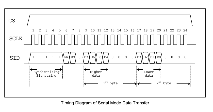
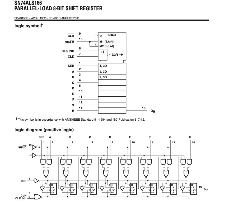
Visual examination and Passive probing with a multimeter shows that the 2 (7 segment leds) are multiplexed with each drive pin being toggled between each display alternatively. The chip is an 74146 serial to parallel shift register which is how the micro on the main board manages to work this display board with so few connections.

You might wonder why I am taking so much interest in this board?

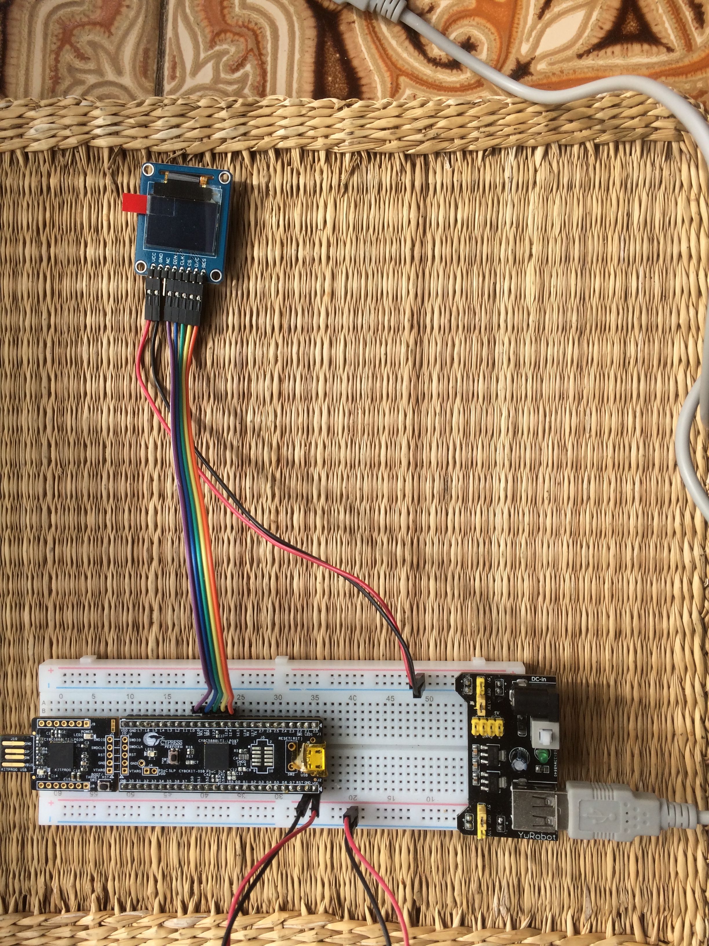
The board is the only way to set motor speed and direction and is a bit of pain to do so. So I  intend to read and send commands to the motor controller via a better display and menu and not have to remember which code is needed to set which parameter.As I started to document this I suddenly realised that I can safely power up and probe the display board just by unplugging it from the main board and then powering it up in the electronics lab with my trusted bench power supply and attach patch pins and probes, as I want, without causing a short of the 0v line down to ground. Its a rainy day so this is a good option to get on with.
Working from the top connections.Pin 1 marked + is 5 volt dc from the main board.Pin 2 UP switch 20k ohm to + volts and connected to -V when pressed.Pin 3 DOWN switch similar electrical connection as UP switch.Pin 4 CLOCK for 74146 serial connection.Pin 5 Led 7 segment display select line.Pin 6 A&B data input for 74146 serial connection. Pin 7 marked – is 0 volt dc from main board.
The display board powers up from the bench supply with about 1 mA being drawn by each segment of a display.
I can now define that:-Pin 2 and Pin 3 push buttons go High 5V when pressed which is closed or make, held low 0V when open and not made.Pin 5 led display selector when at 0V selects right digit, with 5V left digit selected. Pin 4 clock and Pin 6 data are driven at normal TTL input levels.
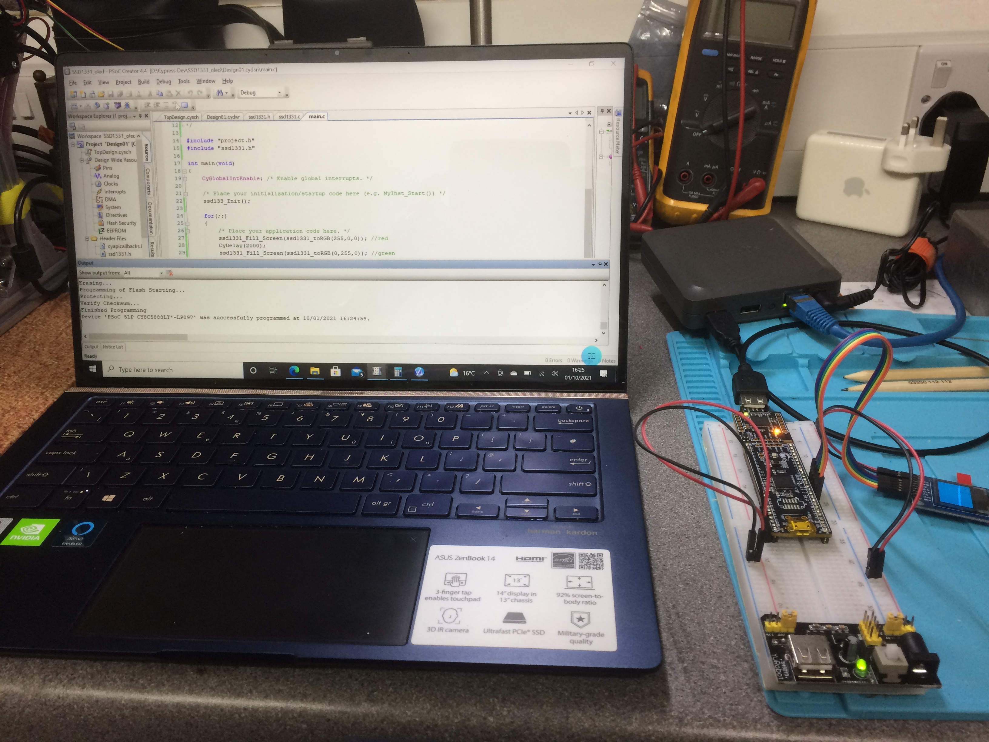
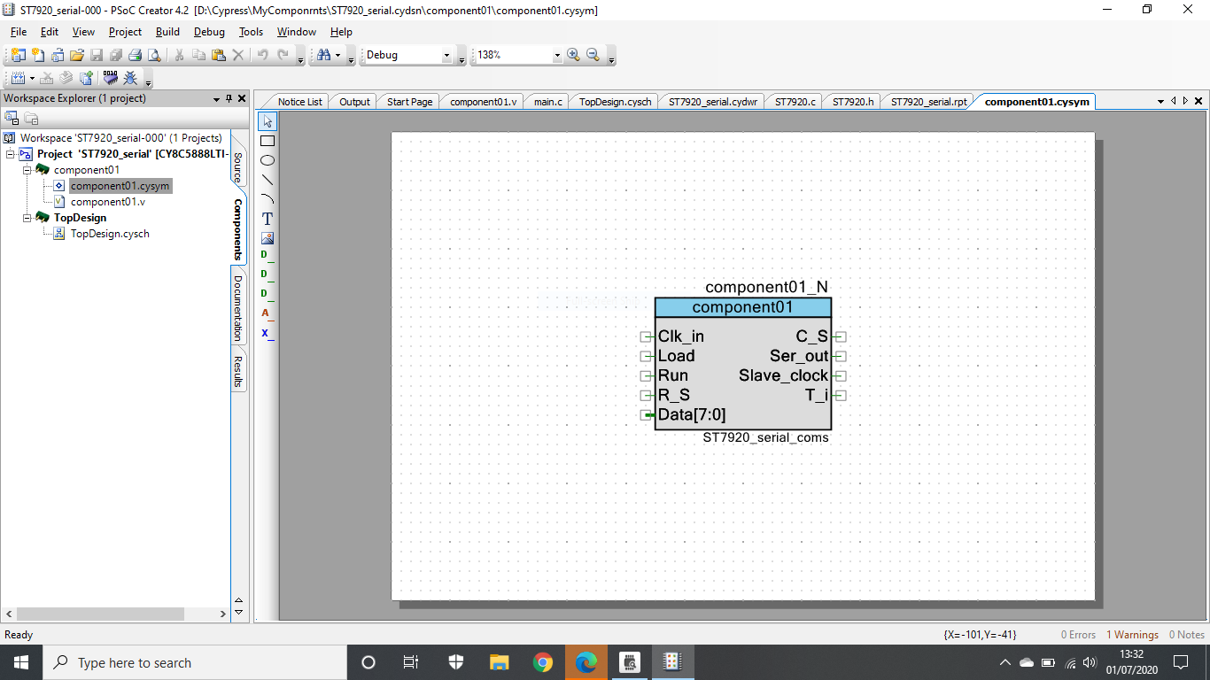
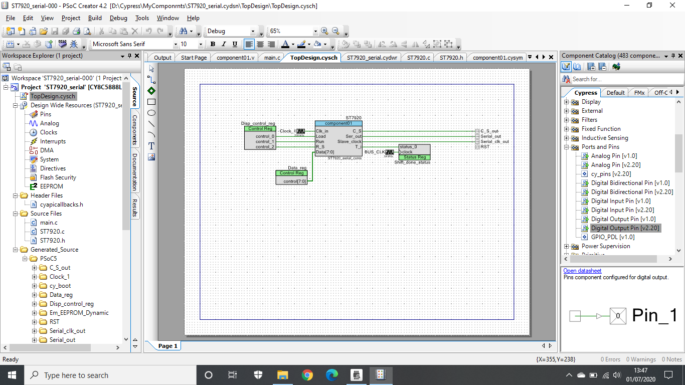
I am not sure what the main board processor can output on a pin so I will use a TTL buffer to drive the opto-coupler which needs 10 mA for full turn on of the opto isolated output transistor. I have started on a design in Kicad. This design has been exported from the Kicad schematic to VeeCad, so that I can get it working first on veroboard before getting a PCB made up. Once the isolation electronics are proven on the bench, I will then work out the serial stream data that is sent to the displays and with the help of a PSoC 5 development board mimic the displays on a HD44780 4 * 20 LCD display.Then it becomes a process of writing some code on the PSoC to activate the buttons electronically for different speeds and rotations required on the motor.Back to mechanics I have the 32mm bore timing gear for the headstock drive shaft and have made a new aluminium 32mm bore spacer to get the lead screw drive gear in the right position along with the timing drive gear. The motor has a V belt pulley with a 15mm bore, the new timing gear for this has pilot hole and needs to be bored out to 15mm and awaits the arrival of a 15 mm drill. The original V pulley has a Woodruff key, so the new gear will need a set screw to stop rotation or possibly a slot for the Woodruff key? I finally opt for a hex key grub screw drilled and tapped into the timing gear.I intend to get the whole unit mounted together and then run the bearing a shaft in for a bit on the bench, before fitting on the lathe. I can monitor bearing temperature and play easily along with getting some idea of the turning speeds I will be able to programme and control with the speed lever.
I have the motor mounted and everything linked so the headstock got fitted today and powered up on the lathe. Turned a bit of brass rod on the lathe and its the surface finish is the best I have had to date the cross cut is a mirror finish and the transverse cut is good but a little rough may need a new cutter and or the mechanical feed brought on line. I am having to modify the gear plate for the mechanical feed to the cutter as the belt is a lot wider than the original. However the belt is a standard stock option and cheap as well as being powerful.

I also need to look at home build isolated probes for my scope???

PSoC and SSD1331 oled display

SSD1331 RGB oled display 0.95 inch SPI Full Colour OLED Display SSD1331 96X64

Now you will see plenty of these displays on the web sold as Arduino experimental displays and they all use the very great resources found in the Arduino world.

Many of you know I like PSoC devices and especially the very useful CY8CKIT-059 PSoC® 5LP Prototyping Kit With Onboard Programmer and Debugger

Images from this site

So it will come as no surprise that I have decided to get this development board talking to the SSD1331 display. This is especially pertinent for me as I am writing a series of display drivers with a common graphics core. There are plenty of graphics cores available free on the web, but they all seem to take a large amount of effort to implement in C99 code, which is the favoured programming language of CREATOR the free programming resource and IDE that comes with these development kits.

The secret with the SSD display drivers is having the right initialisation code for the display so in the first part of this blog I am going to build the initialisation code in CREATOR.

At this point I am going to thank PAUL STARON for allowing me to use and blog about his code for the SSD1331 display he has on ARM mbed. I will be mangling and changing his code to suit my code style and the PSoC Creator C99 code environment. So complain to me about any code faults in this blog, Paul is innocent.

First thing that is needed before anything can happen is to configure the SPI hardware that will be used to drive the display. This is manly a drag and drop activity in Creator and is shown below.

Creator IDE placing a SPI Master component and named output pins

It is also a good thing to setup all the outputs to the display and get the order of the output pins of the CY8CKIT-059 development kit to match the order of input pints to the display so that a flat ribbon cable can make the link between the two units.

Creator IDE assigning output pin names to CY8CKIT-0.59 dev board hardware port

Be aware that the display as sold is expected to be run on 3.3volts it will take 5volts but I do not know for how long they will work at this voltage. As the CY8CKIT-059 development kit is programmed at USB 5volt I have taken the precaution of running the display with a 3,3volt module using the E-Bay plug in power supply and just keeping output pins at 5volt while programming. and modifying code.

All the hardware done now just the code to get going.

Header(.H)

/* ========================================
 *
 * Copyright Crusty Consultants, 2021
 * All Rights Reserved
 * PUBLISHED, SOFTWARE.
 * Main Contributor "Paul Staron" from public published work on "Mbed"
 * Ported to PSoC by Crusty Consultants.
 * Please acknowledge the above if using for publication or production.
 * No warranty is provided for the functioning of this software.
 * Used at own risk.
 * ========================================
*/

#ifndef __SSD1331_H__
    #define __SSD1331_H__
     
    #include "project.h"
     
    // Screen Settings
    #define width   96-1        // Max X axial direction in screen
    #define height  64-1        // Max Y axial direction in screen
    #define Set_Column_Address  0x15
    #define Set_Row_Address     0x75
    #define contrastA           0x81
    #define contrastB           0x82
    #define contrastC           0x83
    #define display_on          0xAF
    #define display_off         0xAE
     
    // Internal Font size settings
    #define NORMAL  0
    #define WIDE    1
    #define HIGH    2
    #define WH      3
    #define WHx36   4
    #define X_width 6 
    #define Y_height 8 
     
     
    // GAC hardware acceleration commands
    #define GAC_DRAW_LINE           0x21    // Draw Line
    #define GAC_DRAW_RECTANGLE      0x22    // Rectangle
    #define GAC_COPY_AREA           0x23    // Copy Area
    #define GAC_DIM_WINDOW          0x24    // Dim Window
    #define GAC_CLEAR_WINDOW        0x25    // Clear Window
    #define GAC_FILL_ENABLE_DISABLE 0x26    // Enable Fill
    #define SCROLL_SETUP            0x27    // Setup scroll
    #define SCROLL_STOP             0x2E    // Scroll Stop
    #define SCROLL_START            0x2F    // Scroll Start
     
    // Basic RGB color definitions         RED GREEN BLUE values                         
     
    #define Black           0x0000      //   0,   0,   0 
    #define LightGrey       0xC618      // 192, 192, 192 
    #define DarkGrey        0x7BEF      // 128, 128, 128 
    #define Red             0xF800      // 255,   0,   0 
    #define Green           0x07E0      //   0, 255,   0 
    #define Cyan            0x07FF      //   0, 255, 255 
    #define Blue            0x001F      //   0,   0, 255 
    #define Magenta         0xF81F      // 255,   0, 255 
    #define Yellow          0xFFE0      // 255, 255,   0 
    #define White           0xFFFF      // 255, 255, 255 
 
// Public functions
    void ssd133_Init(void);
    void ssd1331_cls();
    uint16_t ssd1331_toRGB(uint16_t R,uint16_t G,uint16_t B);
    void ssd1331_Fill_Screen(uint16_t color);
    void ssd1331_fillrect(uint8_t x1,uint8_t y1,uint8_t x2,uint8_t y2,uint16_t colorline,uint16_t colorfill);
#endif

/* [] END OF FILE */

Source(.C)

/* ========================================
 *
 * Copyright Crusty Consultants, 2021
 * All Rights Reserved
 * PUBLISHED, SOFTWARE.
 * Main Contributor "Paul Staron" from public published work on "Mbed"
 * Ported to PSoC by Crusty Consultants.
 * Please acknowledge the above if using for publication or production.
 * No warranty is provided for the functioning of this software.
 * Used at own risk.
 * ========================================
*/

#include <ssd1331.h>

// private variables
    uint16_t Char_Color;    // text color
    uint16_t BGround_Color; // background color
    uint8_t chr_size;       // size character to be set at.
    
//private functions specific to ssd1331.c

// Communication functions to commuinicate with Display SPI interface.
// Note CS pin raised and lowered by component along with data and clock timing for each 8 bit byte sent.

    void  ssd1331_RegWrite(unsigned char Command)
    {
        
        DC_Write(0);     // set the display pin D/C pin to low as this is a command
        SPIM_1_WriteByte(Command);//send the command value
    };

    void  ssd1331_RegWriteM(unsigned char *Command, uint8_t count)
    {
        int i;
        DC_Write(0);     // set the display pin D/C pin to low as this is a command
        for( i=0; i<count; i++) {
            SPIM_1_WriteByte(*Command++);//send a series of commands
        }
    }

    void  ssd1331_DataWrite(unsigned char c)
    {
        DC_Write(1);    // set the display pin D/C pin to high as this is DATA
        SPIM_1_WriteByte(c);
    }

    void  ssd1331_DataWrite_to(uint16_t Dat)
    {
        DC_Write(1);    // set the display pin D/C pin to high as this is DATA    
        SPIM_1_WriteByte((unsigned char)((Dat >> 8)));
        SPIM_1_WriteByte((unsigned char)(Dat));
    }
    
//public functions
    void ssd1331_Maxwindow()
    {    
        unsigned char cmd[7]= {Set_Column_Address,0x00,0x5F,Set_Row_Address,0x00,0x3F};
        ssd1331_RegWriteM(cmd, 6);
    }
    
    void ssd1331_foreground(uint16_t color)
    {
        Char_Color = color;
    }
    
    void ssd1331_background(uint16_t color)
    {
        BGround_Color = color;
    }
    
    void ssd1331_cls()
    {
        unsigned char cmd[6]= {GAC_CLEAR_WINDOW,0,0,width,height};
        ssd1331_RegWriteM(cmd,5);
        CyDelay(500);
        ssd1331_Maxwindow();
        ssd1331_background(Black);//
    }
    
    uint16_t ssd1331_toRGB(uint16_t R,uint16_t G,uint16_t B)
    {  
        uint16_t c;
        c = R >> 3;
        c <<= 6;
        c |= G >> 2;
        c <<= 5;
        c |= B >> 3;
        return c;
    }
    
    void ssd1331_fillrect(uint8_t x1,uint8_t y1,uint8_t x2,uint8_t y2,uint16_t colorline,uint16_t colorfill)
    {
        if  ( x1 > width ) x1 = width;
        if  ( y1 > height ) y1 = height;
        if  ( x2 > width ) x2 = width;
        if  ( y2 > height ) y2 = height;
     
        unsigned char cmd[11]= { 0 };
        cmd[0] = GAC_FILL_ENABLE_DISABLE;
        cmd[1] = 1;      // fill 1, empty 0
        ssd1331_RegWriteM(cmd, 2);
        cmd[0] = GAC_DRAW_RECTANGLE;
        cmd[1] = (unsigned char)x1;
        cmd[2] = (unsigned char)y1;
        cmd[3] = (unsigned char)x2;
        cmd[4] = (unsigned char)y2;
        cmd[5] = (unsigned char)((colorline>> 11) << 1);    // Outline Blue
        cmd[6] = (unsigned char)((colorline>> 5 ) & 0x3F);  // Outline Green
        cmd[7] = (unsigned char)((colorline<< 1 ) & 0x3F);  // Outline Red
        cmd[8] = (unsigned char)((colorfill>> 11) << 1);    // fill Blue
        cmd[9] = (unsigned char)((colorfill>> 5 ) & 0x3F);  // fill Green
        cmd[10]= (unsigned char)((colorfill<< 1 ) & 0x3F);  // fill Red
        ssd1331_RegWriteM(cmd, 11);
        CyDelayUs(500);
    }
    
    void ssd1331_Fill_Screen(uint16_t color)
    {
        BGround_Color = color;
        ssd1331_fillrect(0,0,width,height,color,color);
    }
    
    void ssd133_Init(void)
    {

        SPIM_1_Start(); //activate the spi master component
        // reset
        CyDelay(200);
        RES_Write(0);       //Reset active
        CyDelay(200);
        RES_Write(1);       // reset released
        CyDelay(200);       // wait 200mS for display processor to settle
     
        // initialize sequence
        ssd1331_RegWrite(0xAE);    //OLED display OFF
        ssd1331_RegWrite(0x75);    /* Set Row Address */
        ssd1331_RegWrite(0x00);    /* Start = 0 */
        ssd1331_RegWrite(0x3F);    /* End = 63 */
        ssd1331_RegWrite(0x15);    /* Set Column Address */
        ssd1331_RegWrite(0x00);    /* Start = 0 */
        ssd1331_RegWrite(0x5F);    /* End = 95 */
        ssd1331_RegWrite(0xA0);    //Set remap & data format 0111 0000
        ssd1331_RegWrite(0x72);    // RGB colour
        ssd1331_RegWrite(0xA1);    //set display start row RAM
        ssd1331_RegWrite(0x00);
        ssd1331_RegWrite(0xA2);    //set dispaly offset
        ssd1331_RegWrite(0x00);
        ssd1331_RegWrite(0xA4);    //Set Display Mode
        ssd1331_RegWrite(0xA8);    //Set Multiplex Ratio
        ssd1331_RegWrite(0x3F);
        ssd1331_RegWrite(0xAD);    //Set Master Configuration
        ssd1331_RegWrite(0x8F);    //(External VCC Supply Selected)
        ssd1331_RegWrite(0xB0);    //Set Power Saving Mode
        ssd1331_RegWrite(0x1A);
        ssd1331_RegWrite(0xB1);    //Set Phase 1 & 2 Period Adjustment
        ssd1331_RegWrite(0x74);
        ssd1331_RegWrite(0xB3);    //Set Display Clock Divide Ratio / Oscillator Frequency
        ssd1331_RegWrite(0xD0);
        ssd1331_RegWrite(0x8A);    //Set Second Pre-charge Speed of Color A
        ssd1331_RegWrite(0x81);
        ssd1331_RegWrite(0x8B);    //Set Second Pre-charge Speed of Color B
        ssd1331_RegWrite(0x82);
        ssd1331_RegWrite(0x8C);    //Set Second Pre-charge Speed of Color C
        ssd1331_RegWrite(0x83);
        ssd1331_RegWrite(0xBB);    //Set Pre-charge Level
        ssd1331_RegWrite(0x3E);
        ssd1331_RegWrite(0xBE);    //Set VCOMH
        ssd1331_RegWrite(0x3E);
        ssd1331_RegWrite(0x87);    //Set Master Current Control
        ssd1331_RegWrite(0x0F);
        ssd1331_RegWrite(0x81);    //Set Contrast Control for Color gAh
        ssd1331_RegWrite(0x80);
        ssd1331_RegWrite(0x82);    //Set Contrast Control for Color gBh
        ssd1331_RegWrite(0x80);
        ssd1331_RegWrite(0x83);    //Set Contrast Control for Color gCh
        ssd1331_RegWrite(0x80);
        ssd1331_RegWrite(0xAF);    //display ON
     
        chr_size = NORMAL;
        ssd1331_cls();
    }
/* [] END OF FILE */

Main

/* ========================================
 *
 * Copyright Crusty Consultants, 2021
 * All Rights Reserved
 * PUBLISHED, SOFTWARE.
 * Main Contributor "Paul Staron" from public published work on "Mbed"
 * Ported to PSoC by Crusty Consultants.
 * Please acknowledge the above if using for publication or production.
 * No warranty is provided for the functioning of this software.
 * Used at own risk.
 * ========================================
*/

#include "project.h"
#include "ssd1331.h"

int main(void)
{
    CyGlobalIntEnable; /* Enable global interrupts. */

    /* Place your initialization/startup code here (e.g. MyInst_Start()) */
    ssd133_Init();

    for(;;)
    {
        /* Place your application code here. */
        ssd1331_Fill_Screen(ssd1331_toRGB(255,0,0)); //red
        CyDelay(500);
        ssd1331_Fill_Screen(ssd1331_toRGB(0,255,0)); //green
        CyDelay(500);
        ssd1331_Fill_Screen(ssd1331_toRGB(0,0,255)); //blue
        CyDelay(500);
        ssd1331_Fill_Screen(ssd1331_toRGB(255,255,255)); //white
        CyDelay(500);
    }
}

/* [] END OF FILE */
Programming the CY8CKIT-0.59 dev board and running the display

I try not to take chances when programming (like blowing up the computer from short circuits) so I programme the dev board by a remote USB network device. This also gets rid of a common ground between the PC and the dev board.

Because I am mean this is not showing the MOV file I took of the ever changing screen block colours. however click on this link to see the actual sequence

Have moved the site to PSoC Crusty Hacks Including (Crusty Bits) as I seem to be able to get on better with the editor software there.http://crusty-hacks-psoc.blogspot.com

ST7920 128 x 64 Graphics and text display using SPI and Cypress PSoC custom component.

Image

So it’s been a bit of a long time since I blogged on WordPress, but I am back again. Please bear with this specific blog as it is a work in progress.

Also apologies for layout glitches as I am getting used to the new blocks editor on WordPress before they retire the old WYSIWYG editor.

I had an old WG12864a display in my components box and I wanted to get it working with one of my PSoC development boards.

Sadly the magic grey smoke has escaped from both the display and the development board when an errant flying wire contacted with something it should have stayed away from.

Never fear this handy trader on E-Bay had a similar Text and Graphic Display using the ST7920 display driver.

There are lots of Arduino sketches for these types of display, but not much for Cypress PSoC 4 & 5 devices. As you will all know by now Crusty of “Crusty Hacks” likes the programmable hardware PSoC chips use. Using programmable hardware to handle what would b a “bit bashing” fest on a micro makes an awful lot of sense to me and being able to do things in parallel without intervention of the embedded micro just seems right.

So there are a number of options when using this display 4 bit, 8 bit and SPI modes of communication

  • 4 bit mode will use 8 pins on the controller,.
  • 8 bit uses 12 pins.
  • SPI uses 4 pins.

There are I2C breakout boards that provide a I2C serial to parallel mode for these displays, which will use only 3 pins from the controller. SPI uses 3 but I have opted to add one extra pin to allow for a hardware rest line.

The SPI data that is sent to the display is write only and is made up of 24 bits of data, only 9 bits of data will change in any 24 bit data frame, RW bit (Read/Write) will always be write as there is no read capability in SPI mode. Only the RS bit (Command or Data) and the 4 Higher and 4 Lower bits of data are going to change in any data frame.

Diagram from Sitronix data sheet.

Untitled.png
page26image26865280
This got me to thinking that all I need is a shift register that I can load with 8 bits of data and one RS bit (Command Zero or Data one), all the other bits are constantly assigned to the relevant bits of a 24 bit serial shift register. Easy or Hard?
 
Cypress PSoC Creator has a 24 bit shift register already prebuilt. Just drag and drop it into a schematic job done, well not quite.The shift register has to be loaded each time with all 24 bits of data and I just want to be a tech and load 9 bits of data for each frame.
I am also thinking of using the display on a Xilinx FPGA board and the early chips do not come with a processor built in.

It’s time to build a custom component for my Cypress PSoC 5 development board.

I am going to learn enough Verilog HDL (High Level Description language) to get Cypress Creator Warp Verilog to synthesise the component for me. 

The component is going to need  CLOCKS 

  • An input clock
  • A data clock to drive the data out one bit at at time from the SID output
  • A SCLK output that is 90 degrees out of phase with the data stream so the display knows when to read the data.

The component is going to need  inputs.

  • 8 data inputs.

The component is also going to need outputs.

  • outputI SCLK output
  • 1 CS output

The component is also going to need control inputs and outputs

  • 1 Load control line.
  • 1 Run control line.
  • 1 Frame sent or ready to load control line.

Now this is looking like a lot of inputs and outputs, but the component being designing is in the PSoC chip and only has the SID, SCLK and CS outputs coming out of the physical pins of the PSoC 5 chip. 

Screen Shot of the component thats needed

Component.PNGNext thing to do is think about what we want to happen.

  • Take an input clock make two clocks in step with each other but 90 degrees out of phase, Not as difficult as you might think only 2 d flip flops and some inverters. Diagram from

  • The parallel load serial shifter element is needed but it’s going to be 24 bit long and not 8 bit as per the diagram taken fromTexas Instruments Data sheet.

Screenshot 2020-06-30 at 15.14.11There is a slight flaw in my decision to use Warp Verilog to make my component

Warp Verilog needs you to be conversant with writing Verilog already, you input the Verilog just as you might write a C file. The error messages when Warp copies are not very helpful Warp has no RTL diagrams or Schematic diagrams and no testbed feature.

I have hit this before and have found a way to use the old but excellent Xilinx FPGA’s ISE design suite to write Verilog instructions that can be cut and pasted in to the Creators Warp Verilog file. The reason I use ISE is that it has an embedded help which has snippets of code for just about every element that you will use in your Verilog code, which you can copy and paste. It also has a schematic capture option which is not quite as useful for what we are going to do.

ISE is a big programme and you need a fairly fast PC, however you are not working in the cloud. While learning you can keep recompiling as often as you need to get rid of all the syntax errors and logic errors you may have. Now half the learning cycle of Verilog or even (VHDL) is understanding the error messages during synthesis. Whats “SYNTHESIS” in my simple terms getting your text description of the circuits components and their timing interaction transferred into logic packages the the FPGA vendor can assemble in the undedicated logic on their chip. This is where the fun starts take the simple logic function that we will use in our component.

This will synthesise into the following schematics

Registerter-transfer level RTL schematic.

Technology schematic   

So this is what Xilinx would fabricate the circuit as.

Interestingly the Xilinx Technology design has got rid of the simple flip-flops and used a flip-flop with a clear and reset. Similarly when we use the Verilog description in the Creator WARP file then we are told that WARP will parse the Verilog description and utilise predefined components in WARP to generate our design.

Which is why I put a logic analyser on the outputs and inputs of a custom component so that I can see that the design performs as expected.

The Module used in a Creator Schematic design

Component diagram

The Verilog HDL that sits inside the component above

include “cypress.v”
//`#end` — edit above this line, do not edit this line
// Generated on 06/23/2020 at 12:10
// Component: component01

module component01 (
output reg C_S,
output  Ser_out,
output reg Slave_clock,
output reg T_i,
input   Clk_in,
input  [7:0] Data,
input  wire Load,
input   R_S,
input  wire Run
);
//`#start body` — edit after this line, do not edit this line

//        Your code goes here
reg [23:0] shifter;
assign Ser_out = shifter[23];// set this as the output buffer
reg running;
reg [4:0] count; //set up the incrimenting counter for counting bits shifted
//**************take clock in signal divide by 2 and generate two clocks shifted by 90 degrees************
reg a;
reg b;
     wire Clk_0; 
     assign Clk_0 = a;
     wire Clk_90;
     assign Clk_90 = b;

always @ (posedge Clk_in)
begin
a <=~a;
end

always @ (negedge Clk_in)
begin
         if(running == 1’b1)
         begin
    b <= ~b;
            Slave_clock <= Clk_90;
         end else
         begin
            Slave_clock <= 1’b0;
         end
end

//***************************************************** 

always @ (posedge Clk_0)
begin
if(Load == 1 )
begin
shifter[23:19]<=5’b11111;//low value to start in bit 24 followed by 5 framing ones
shifter[18]<=1’b0;
shifter[17]<=R_S;
shifter[16]<=1’b0;
shifter[15:12]<= Data[7:4];
shifter[11:8]<=4’b0000;
shifter[7:4]<= Data[3:0];
shifter[3:0]<=4’b0000;
T_i <=1’b0;
C_S <=1’b0;
count <=5’b00000;
running <=1’b0;//set slave clock off
end
else
if(Run == 1 )
begin
           if(count == 0)
           begin
                C_S <= 1’b1;// set Chip select high
                running <= 1’b1;//set up the reg to start Slave_clock //output(always(negedge Clk_in)statement
                T_i <= 1’b0;
                count <= count + 1;//increment count so this only act s once
           end
  if(count >= 1 & count <=23)
begin
shifter <= shifter <<1;// move bits to the right and out to  output with shifter[24} as Ser_out pin
count <= count +1;//keep a count of how many times shift happens
end
else if(count > 23)//sent all the serial bits
begin
C_S <=1’b0;//Chip select goes low
T_i <=1’b1;
running <= 1’b0;//set up the reg to stop Slave_clock output(always(posedge Clk_in)statement)
end
end

end
//`#end` — edit above this line, do not edit this line
endmodule
//`#start footer` — edit after this line, do not edit this line
//`#end` — edit above this line, do not edit this line

Had a bit of trouble adding a testbed so below is the screenshot for the the initialising  sequence for the display.Capture
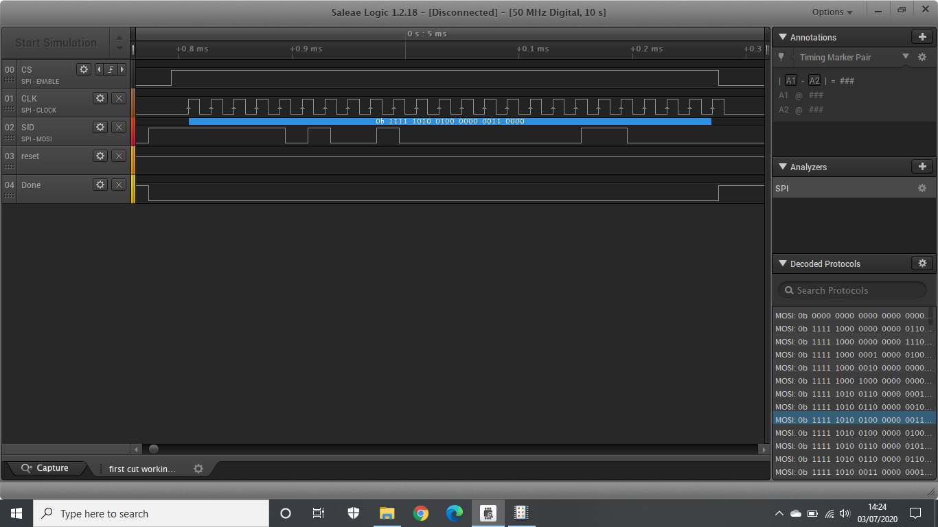
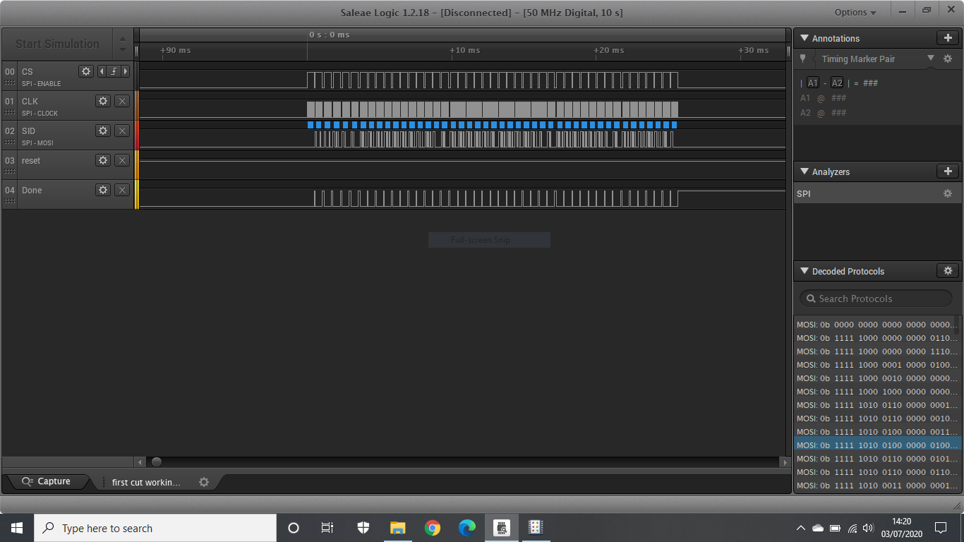
And here is the screen shot of one 24 bit serial frame sent to the display.Capture 2

Now the H file of what will become the API for the module


#include <project.h>
#ifndef __ST7920_H__
#define __ST7920_H__

#include <stdbool.h>
#include <string.h>
#define ACTIVE 1
#define INACTIVE 0
#define COMMAND 0
#define DATA 1
#define RESET_ACTIVE 0
#define RESET_INACTIVE 1


void ST7920_hard_reset();
void ST7920_basic_instruction();
void ST7920_disply_clear();
void ST7920_command_data( uint8 command_data, uint8 c_d_byte);
void ST7920_write_character(uint8 line, uint8 position ,char character);
void ST7920_write_string(uint8 line, uint8 position ,char *string_out);

#endif

/* [] END OF FILE */

The C File that will become the API of the Module

#include <ST7920.h>

int modifyBit(int x, unsigned char position, bool newState)
{
int mask;
int state;

mask = 1 << position;
if (newState == 1) state = 1; else state = 0;// relies on true = 1 and false = 0
return (x & ~mask) | (-state & mask);
}

void ST7920_command_data( uint8 command_data, uint8 c_d_byte)
{

// bits 0load, 1run, 2R_S
//should cope with what ever clock is set for the serial component
uint16 command_delay = 1600;//longest delay used
// while(Shift_done_status_Read() == 0)
{
//do nothing a previous shift is in process
};
Disp_control_reg_Write(0b00000000);//shifting has stopped now, control reg value should hold component stopped
Data_reg_Write(c_d_byte);//set up the c-d_byte to send out
if (command_data == COMMAND)
{
Disp_control_reg_Write(0b00000001);//load with register select bit 2 as command 0
while(Shift_done_status_Read() != 0){}; // wait for the load to complete slow clock shown by Ti output on comonent going high
Disp_control_reg_Write(0b00000010);//run, register select dont care in run mode as loaded
if(c_d_byte == 0b00000010)
{
command_delay = 1600;//clear screen takes a long time
}
else
{
command_delay = 200;//most other commands
}
};
if (command_data == DATA)
{
Disp_control_reg_Write(0b00000101);//load with register select bit 2 as data 1
while(Shift_done_status_Read() != 0){}; // wait for the load to complete slow clock Ti of component going low
Disp_control_reg_Write(0b00000110);//run, register select dont care in run mode as loaded
command_delay = 50;//delay for data to be stored.
};
while(Shift_done_status_Read() == 0){};//do nothing until shift complets
CyDelayUs(command_delay);//delay for display processor to complete action

};
/*
void ST7920_data(uint8 data_byte)
{
// bits 0load, 1run, 2R_S
Disp_control_reg_Write(0b00000000);//should hold stopped
Data_reg_Write(data_byte);//set up the command byte to send out
Disp_control_reg_Write(0b00000101);//load with register select bit 2 as data 1
Disp_control_reg_Write(0b00000110);//run,RS x dont care register select in run mode as loaded
while (Shift_done_status_Read() == 0)//check to see when all serial data sent
{
};
CyDelayUs(2000);//delay for data to be stored.
};
*/
void ST7920_basic_instruction()
{
ST7920_command_data(COMMAND,0b00000110);//cursor moveto the right DDRAM address counter (AC) plus 1
ST7920_command_data(COMMAND,0b00001110);//Display on,cursor on,blink off
ST7920_command_data(COMMAND,0b00010100);//cursor mover right by 1 position
ST7920_command_data(COMMAND,0b00100000);//4bit bus (should be dont care basic instruction set
};

uint8 ST7920_set_DDRAM_address(uint8 line, uint8 position)
{
uint8 DDRAM_add =0;
switch(line)
{
case 0 : DDRAM_add = 0x80; break;
case 1 : DDRAM_add = 0x90; break;
case 2 : DDRAM_add = 0x88; break;//yes correct data sheet wrong
case 3 : DDRAM_add = 0x98; break;//yes correct data sheet wrong
};
DDRAM_add = DDRAM_add + (position / 2);
ST7920_command_data(COMMAND,DDRAM_add);
return(DDRAM_add);
};

void ST7920_write_character(uint8 line, uint8 position ,char character)
{
ST7920_set_DDRAM_address(line,position);
ST7920_command_data(DATA,character);

};

void ST7920_write_string(uint8 line, uint8 position ,char *string_out)
{
uint8 count = 0;
ST7920_set_DDRAM_address(line,position);
for(count = 0; count <= strlen(string_out); count ++)
{
ST7920_command_data(DATA,string_out[count]);
};
};

void ST7920_hard_reset()
{
RST_Write(0);
CyDelay(100);//wait
RST_Write(1);
CyDelay(200);//wait
ST7920_command_data(DATA,0b00000000);//reset the serial component to quiescent state dummy data send
ST7920_disply_clear();
};

void ST7920_disply_clear()
{
ST7920_command_data(COMMAND,0b00000001);//display clear
};


/* [] END OF FILE */

I have just started on the basic C functions to support the graphic display and this will have a 5*7 ascii font.So given the Covid19 keeps me indoors there should be some more code added to this blog along with basic lines squares and circles, which actually means adapting previous code for a SSD1331 display. So I will try not to keep you waiting too long.

Getting text to format in the correct position on a line

Text should be easy to send except that the display has really been set up to display Chinese characters which are 16 x 16 character fonts, but will display two 16 * 8 ascii characters which means there are only 8 write locations in a 16 character line.

I took the easy way out to handle formatting a line of text, especially as you can not read memory from the display in serial mode. I am using four arrays of 16 char elements to represent line0 ,1 ,2 ,3 of the text display. On each edit of a line I edit the Array, to position the characters being sent and then just send the whole line array to the display. This way I can edit numbers theatre scaling up and down without affecting the text in the line. Oh there was a “got yer ” in the data sheets memory map for text line start address which I have itemised in the software driver for outputting text. Which is why I have been so slow in putting a video of the text in the blog.

ST7920 Graphics addressing is wierd.

THE GAMES AFOOT.

AS for graphics yet again this has driven me to distraction, as the data sheet is not that clear how the blocks of 16pixels are stored to the screen.

It turns out that the display only has a Vertical Y address of 32 lines and the Horizontal X address is 8 blocks of 16 bits for the upper half of the display. For the lower half you need the Vertical Y (0-63 lines) as modulo of 32 and then add 8 to the Horizontal X address blocks of 16bits.

along the way the MSB needs to be the LSB in the 16 bits of a block. I will include the hack of my code for the graphics and text tomorrow with a video of it in action.

I very nearly have enough of this working now to go onto my next part of the project which is the next blog


CYPRESS PSoC 4 controlling an HD44780 LCD display via I2C Port extender

https://plus.google.com/u/0/100845918259366165719/posts/eebbwZDWRiM?pid=6135734277326915362&oid=100845918259366165719

Ok so this is the code that I use to run an I2C AD8574 8 bit expansion port with an HD44780 LCD 4 line by 20 character display. all this is driven by a standard Cypress PSoC 4 development board link to video of this working on an earlier version of code

The following C code is free to all to use but I take no responsibility for how it works on your equipment.

I will however talk about what I have done to the point of boredom.

Have fun the C code below is compiled from a huge amount of information on the web most reasons for the displays not working is not providing a long enough wait state between commands and the strange way the display memory is addressed.


/* ========================================
*
* Copyright Crusty Consultants, 12/11/2015
* All Rights Reserved
* PUBLISHED, Free to use and abuse SOFTWARE.
*
* If it does not work then it’s not my fault
* I will explain what I have done if any one interested.
* This is part of a bigger works in progress to make solid state disk drives for older computers
* hence the comment about BBC B disc drive
* ========================================
*/
#include <project.h>
#include <stdbool.h>
#include <stdio.h>
uint8 const SlaveAdd8574   = 0x20;
uint8 const SlaveAdd8574A  = 0x70;//probably wrong
uint8 const HD44780I2C = 0x27;
uint8 const DisplayWidth = 20;
uint8 SlaveAdd;

bool Instruction = false; //low instruction input
bool Data = true; // Hi Data input
bool Write = false;// R/W low Write
bool Read = true;// R/W  hi Read
bool E_Inactive = false;// Enable low not enabled
bool E_Active = true;// Enable  hi Enabled
bool BL_On = true;
bool BL_Off = false;
bool Track_Changed = false;
uint8 const R_S = 0;
uint8 const R_W = 1;
uint8 const E   = 2;
uint8 const BL  = 3;
uint8 const StepDir = 1;//bit 1
uint8 const StepPulse = 0;//bit 0
uint8 const Line0 = 0x00;
uint8 const Line1 = 0x40;
uint8 const Line2 = 0x14;
uint8 const Line3 = 0x54;
uint8 BackLight;
uint8 Track_Count;

uint8 SetBitState8(uint8 SourceVal, uint8 BitPos,bool BitStateReq );
void Write_Port(uint8 OutVal);
void Write_LCD(uint8 Register,uint8 SendNibble);
void Enable_4bit();
void WriteMessage(char Message[]);
void SetLCDLine(uint8 LineNo, uint8 CursorPosition, bool ClearLine);
CY_ISR(Seek_Step_Int);
int main()
{
/* Place your initialization/startup code here (e.g. MyInst_Start()) */
BackLight = BL_On;
SlaveAdd = HD44780I2C;
I2C_Port_Start();
Step_Counter_Start();
Index_Pulse_Start();
char msg[] = “BBC B Disk Emulator”;
Enable_4bit();
WriteMessage(msg);
CyGlobalIntEnable;  /* Uncomment this line to enable global interrupts. */
for(;;)
{
/* Place your application code here. */

};
};
void WriteMessage(char Message[])
{
uint8 HiNibble;
uint8 LoNibble;
uint8 count = 0;
while (Message[count] != 0)
{
HiNibble = Message[count] >> 4;
LoNibble = Message[count] & 0x0F;
Write_LCD(Data,HiNibble);
Write_LCD(Data,LoNibble);
count++;
};
};
void Write_Port(uint8 OutVal)
{
if (BackLight == BL_On)OutVal= SetBitState8(OutVal,BL,BL_On);
I2C_Port_I2CMasterSendStart(SlaveAdd,I2C_Port_I2C_WRITE_XFER_MODE);
I2C_Port_I2CMasterWriteByte(OutVal);
I2C_Port_I2CMasterSendStop();
};

void Write_LCD(uint8 Register,uint8 SendNibble)
{
uint8 ByteToSend = 0;

ByteToSend= SetBitState8(ByteToSend,R_S,Register);//set bit for instruction
ByteToSend= SetBitState8(ByteToSend,R_W,Write);//set bit for write
ByteToSend= ByteToSend | ( SendNibble << 4); // store the nibble to the higher 4 bits and send
Write_Port(ByteToSend);// send without enable to stabalise the port bits
CyDelayUs(10);// let tit stabalise
ByteToSend= SetBitState8(ByteToSend,E,E_Active);//set the enable bit
Write_Port(ByteToSend);;//send the enable
CyDelayUs(10);
ByteToSend= SetBitState8(ByteToSend,E,E_Inactive);//clear the enable bit
Write_Port(ByteToSend);// send the dissable
CyDelayUs(10);

};
void SetLCDLine(uint8 LineNo, uint8 CursorPosition, bool ClearLine)//sets line to 0 to 3 ie 1 to 4
{
uint8 loop;
uint8 HiNibble = 0;
uint8 LoNibble = 0;
uint8 DDRAM = 0x80;// command value for moving cursor in display ram
switch (LineNo)
{
case 0 : DDRAM = DDRAM | Line0;// or first byte of line 0
break;
case 1 : DDRAM = DDRAM | Line1;// or first byte of line 1
break;
case 2 : DDRAM = DDRAM | Line2;// or first byte of line 2
break;
case 3 : DDRAM = DDRAM | Line3;// or first byte of line 3
break;
};
DDRAM = DDRAM + CursorPosition;// add where the cursor should be on line 0- 19
HiNibble = DDRAM  >> 4;
LoNibble = DDRAM & 0x0F;
Write_LCD(Instruction,HiNibble);//
CyDelay(10);
Write_LCD(Instruction,LoNibble);
CyDelay(10);
if (ClearLine == true)
{
for (loop = CursorPosition; loop <=( DisplayWidth – CursorPosition-1) ; loop++)
{
WriteMessage(” “);
}
Write_LCD(Instruction,HiNibble);//Put the cursor back where we want it again
CyDelay(10);
Write_LCD(Instruction,LoNibble);
CyDelay(10);
};
};

uint8 SetBitState8(uint8 SourceVal, uint8 BitPos,bool BitStateReq )
{
if (BitStateReq == true)//want to set the bit at location
{
SourceVal |= 1 << BitPos;
return SourceVal;
};
//not setting so want to clear the bit at bit  location
SourceVal &= ~(1 << BitPos );// want to clear the bit
return SourceVal;

};

void Enable_4bit()
{
CyDelay(20);//first delay on reset or power on
Write_LCD(Instruction,0x03);
CyDelay(5);
Write_LCD(Instruction,0x03);
CyDelay(160);
Write_LCD(Instruction,0x03);
CyDelay(160);
Write_LCD(Instruction,0x02);//enable 4 bit mode
CyDelay(5);
/*function set*/
Write_LCD(Instruction,0x02);
CyDelay(10);
Write_LCD(Instruction,0x08);
CyDelay(10);
/*display off */
Write_LCD(Instruction,0x00);
CyDelay(10);
Write_LCD(Instruction,0x08);
CyDelay(10);
/*display on*/
Write_LCD(Instruction,0x00);
CyDelay(10);
Write_LCD(Instruction,0x0F);
CyDelay(10);
/*Entry Mode*/
Write_LCD(Instruction,0x00);
CyDelay(10);
Write_LCD(Instruction,0x06);
CyDelay(10);
/*clear screen*/
Write_LCD(Instruction,0x00);
CyDelay(10);
Write_LCD(Instruction,0x01);
CyDelay(100);
/*cursor home*/
Write_LCD(Instruction,0x00);
CyDelay(10);
Write_LCD(Instruction,0x02);
CyDelay(100);
};
CY_ISR(Seek_Step_Int)
{
Track_Count = Step_Counter_ReadCapture();
Track_Changed = true;
};

/* [] END OF FILE */

We are on our way.


Fabrication bench in attic workshop

The fabrication bench in a state that is tidy!!, like cooking the bench has to be cleaned down before testing begins ranged on the right are a digital and analogue oscilloscope and the bench power supply.

The multimeter in the tray is cheap and disposable. I can connect it up badly during testing and loss is minimal cost.

Prototype H-Bridge control with Atmel ATTiny85 chip in place

Test circuit may look a little ragged but I only need it to prove that the concept design will work. The grey connector on the right is for programming the chip in the center. White and mauve leads go to the motor on the valve and the red and black to the bench power supply set at 2.7 volts to test everything will work on 2 AA cells that are well discharged.

A look at the plumbing the brass female socket on the left was difficult to find as I kept looking for a coupler and not a socket, once the syntax was correct any number were available the middle connection is made with a male to male hydraulics coupler. all fittings are 3/4 inch BSP (British Standard Pipe).

On test last night and I had the motor cycling back and forth under the control of processor surprisingly the motor is only being activated for  50 microseconds to get it to travel to the end stop in each direction. Have not measured the instantaneous current but bench supply shows around 68 milliamps drawn, this is such a short duration the batteries should last a long time. Standby current is about 3 milliamps and I should be able to get this down to a few microamps by putting the microprocessor to sleep for most of the time.

Hydraulic testing will now have to wait while I have a few days doing some new jobs that have become critical in the bungalow.

However I can now start to work on the final pretty PCB that most people now associate with commercial electronics. I like the idea of the two rotary switches for setting up the water alarm cut off parameters. One will set the flow rate say 10 liters to some other higher figure of liters, the other will set the amount of time in minutes that the set flow can run for, 10 minutes to some higher minute figure. Both switches will have ten stages.

Would it be worth having a display? The next prototype will so I can get debugging information . As I am using a water meter as the flow meter this has the total water consumed, but if I integrate a black box electronic flow meter into the final design then total flow would not be known. Who would the users be? If this went to market in today’s water shortage and water price hikes I suspect most buyers would like total water usage information.

Comments so far are welcomed and if you have extra ideas I will try to combine them.

So long for now.

Hopefully now I have learned a bit more about blogging you may get posts as I update on the day